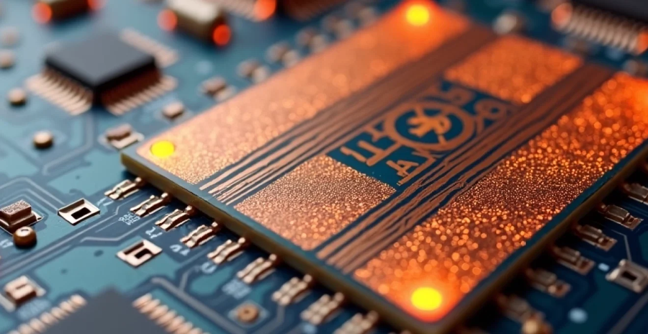
Printed circuit boards (PCBs) are the backbone of modern electronics, providing the foundation for components and connections in countless devices. As technology advances and power requirements increase, engineers and designers are turning to thick copper PCBs as a solution for demanding applications. These specialized boards offer unique advantages that can significantly enhance the performance, reliability, and efficiency of electronic projects.
Thick copper PCBs, also known as heavy copper PCBs, feature copper layers that are substantially thicker than those found in standard PCBs. This increased copper thickness, typically ranging from 3 oz/ft² to over 20 oz/ft², provides a host of benefits that make them an attractive option for various industries and applications. From power electronics to aerospace and automotive systems, thick copper PCBs are making waves in the world of electronic design.
Advantages of thick copper PCBs for electronics projects
The decision to use thick copper PCBs in your next electronics project can bring numerous advantages to the table. These specialized boards offer a combination of electrical, thermal, and mechanical benefits that can significantly improve the overall performance and longevity of your design.
One of the primary advantages of thick copper PCBs is their ability to handle higher current loads. This makes them ideal for power-intensive applications where standard PCBs might struggle or fail. Additionally, thick copper PCBs offer improved heat dissipation, which is crucial for maintaining the stability and reliability of electronic components under demanding conditions.
Another key benefit is the enhanced durability and mechanical strength of thick copper PCBs. This increased robustness makes them well-suited for applications that may be subjected to vibration, shock, or other physical stresses. For industries such as automotive and aerospace, where reliability under harsh conditions is paramount, thick copper PCBs provide an extra layer of assurance.
Furthermore, thick copper PCBs can often simplify design processes by eliminating the need for additional heat sinks or cooling mechanisms. This can lead to more compact and efficient designs, potentially reducing overall system complexity and cost. The icape-group.com provides detailed information on the various advantages and applications of heavy copper PCBs.
Enhanced electrical performance with thick copper circuits
The electrical performance of thick copper PCBs sets them apart from their standard counterparts in several key areas. These improvements can be critical for projects that demand high power handling, precise signal integrity, and minimal voltage drop across conductors.
Increased current carrying capacity in thick copper
One of the most significant advantages of thick copper PCBs is their ability to carry higher currents without overheating. The increased cross-sectional area of the copper traces allows for greater current flow with less resistance. This characteristic is particularly beneficial in power electronics applications, where high currents are the norm rather than the exception.
For example, a 4 oz/ft² copper trace can typically carry about twice the current of a 2 oz/ft² trace of the same width, all other factors being equal. This increased current capacity can lead to more efficient power distribution and reduced energy losses in the form of heat.
Improved signal integrity on thick copper traces
Signal integrity is crucial in high-speed digital circuits and sensitive analog applications. Thick copper traces can offer improved signal integrity due to their lower resistance and inductance. This can result in cleaner signals with less distortion, particularly over longer trace lengths.
The reduced resistance of thick copper traces also means less signal attenuation, which can be particularly beneficial in RF and microwave applications. Engineers working on projects that require precise signal transmission can leverage thick copper PCBs to maintain signal quality and reduce the need for additional signal conditioning components.
Reduced voltage drop across thick copper conductors
Voltage drop across PCB traces can be a significant concern in power distribution networks and high-current applications. Thick copper conductors help mitigate this issue by offering lower resistance paths for current flow. This results in smaller voltage drops across the board, ensuring that components receive the correct operating voltages even under high-load conditions.
The reduced voltage drop can be particularly crucial in battery-powered devices or systems with tight voltage tolerances. By minimizing voltage fluctuations, thick copper PCBs can contribute to more stable and reliable operation of electronic circuits.
Thermal management benefits of thick copper boards
Effective thermal management is a critical aspect of electronic design, particularly as devices become more powerful and compact. Thick copper PCBs offer significant advantages in this area, helping to dissipate heat more efficiently and maintain optimal operating temperatures for components.
Efficient heat dissipation through thick copper layers
The thermal conductivity of copper makes it an excellent material for heat dissipation. Thick copper layers in PCBs act as efficient heat spreaders, quickly moving heat away from components and distributing it across the board. This can help prevent localized hot spots that could potentially damage sensitive components or reduce their lifespan.
In many cases, the heat-spreading capability of thick copper layers can reduce or even eliminate the need for additional heat sinks or cooling solutions. This can lead to simpler, more compact designs without compromising on thermal performance.
Higher power handling capability of thick copper
The increased thermal mass of thick copper PCBs allows them to handle higher power levels without overheating. This characteristic is particularly valuable in applications such as motor controllers, power inverters, and high-power LED drivers, where significant amounts of heat are generated during operation.
By effectively managing heat, thick copper PCBs can allow components to operate closer to their maximum rated power, potentially improving overall system efficiency and performance. This can be especially beneficial in applications where size constraints limit the use of large heat sinks or active cooling systems.
Reduced thermal stress on thick copper PCBs
Thermal cycling, or the repeated heating and cooling of a PCB during operation, can cause significant stress on board materials and solder joints. Thick copper PCBs are better equipped to handle these thermal stresses due to their increased mechanical strength and improved heat distribution properties.
The reduced thermal gradients across thick copper boards help minimize the expansion and contraction that occurs during thermal cycling. This can lead to improved long-term reliability and reduced risk of solder joint failures or board delamination, particularly in applications that experience frequent power cycling or operate in environments with wide temperature variations.
Mechanical strength and durability of thick copper
The mechanical properties of thick copper PCBs contribute significantly to their overall durability and reliability. These boards offer enhanced resistance to physical stresses, making them ideal for applications in harsh environments or those subject to frequent vibration or shock.
The increased copper thickness provides greater structural integrity to the PCB, reducing the risk of trace cracking or separation under mechanical stress. This is particularly important in applications such as automotive electronics, aerospace systems, and industrial equipment, where vibration and shock are common occurrences.
Additionally, thick copper PCBs often exhibit improved resistance to bending and flexing. This can be crucial in applications where the PCB may be subjected to mechanical forces during installation or operation. The enhanced rigidity can help maintain the integrity of solder joints and prevent component displacement, even under challenging conditions.
Another advantage of the mechanical strength of thick copper PCBs is their ability to support heavier components without the need for additional reinforcement. This can simplify board design and assembly processes, potentially reducing overall production costs.
Cost effectiveness considerations for thick copper designs
While thick copper PCBs may have a higher initial cost compared to standard PCBs, they can offer significant cost savings over the lifecycle of a product. Understanding these long-term benefits is crucial when evaluating the cost-effectiveness of thick copper designs for your electronics project.
Long term reliability offsets higher initial costs
The enhanced durability and reliability of thick copper PCBs can lead to reduced maintenance and replacement costs over time. This is particularly valuable in applications where downtime is expensive or where access for repairs is limited or costly.
For example, in industrial automation systems or remote monitoring equipment, the increased longevity of thick copper PCBs can result in fewer service interruptions and lower overall operational costs. The initial investment in a more robust PCB design can pay dividends in terms of reduced maintenance expenses and improved system uptime.
Reduced need for heat sinks saves costs
The superior thermal management capabilities of thick copper PCBs can often eliminate or reduce the need for additional heat sinks or cooling solutions. This not only simplifies the design but can also lead to significant cost savings in terms of materials and assembly time.
In some cases, the cost of a thick copper PCB may be offset by the savings achieved through the elimination of expensive thermal management components. This can result in a more cost-effective overall solution, especially when considering the entire bill of materials for a project.
Extended product life cycle with thick copper
The durability and reliability of thick copper PCBs can contribute to an extended product life cycle. This longevity can be a significant factor in the overall cost-effectiveness of a design, particularly for products that are expected to operate for many years in challenging environments.
By choosing thick copper PCBs, designers can potentially reduce the frequency of product updates or replacements due to PCB failures. This can lead to improved customer satisfaction and reduced warranty claims, further enhancing the cost-effectiveness of the design over its entire lifecycle.
When evaluating the costs associated with thick copper PCBs, it's essential to consider not just the upfront expenses, but also the potential long-term savings and benefits. For many applications, the improved performance, reliability, and longevity offered by thick copper designs can justify the initial investment, resulting in a more cost-effective solution over time.